How to Improve Signal Integrity with Sequential Build Up PCBsAuthor : Adrian September 13,silver solder paste for stainless steel 2025Table of ContentsIn the fast-paced world of electronics, maintaining signal integrity is critical, especially in high-speed PCB design. If you're wondering how to improve signal integrity with sequential build-up PCBs, the answer lies in leveraging their unique layered construction to minimize signal distortion, reduce crosstalk, and control impedance. Sequential build-up (SBU) PCBs, also known as build-up multilayer boards, allow for precise layer stacking and microvia technology, which can significantly enhance performance in high-speed applications. In this comprehensive guide, we'll dive deep into the techniques, benefits, and best practices for using SBU PCBs to ensure optimal signal integrity, helping you design reliable and efficient circuits for modern electronics.
What Is Signal Integrity and Why Does It Matter in PCB Design?Signal integrity refers to the quality and reliability of electrical signals as they travel through a printed circuit board (PCB). In high-speed PCB design, where data rates often exceed 100 MHz or even reach into the gigahertz (GHz) range, maintaining signal integrity becomes a challenge. Poor signal integrity can lead to data corruption, communication errors, and system failures, impacting everything from consumer electronics to aerospace systems. Common issues affecting signal integrity include crosstalk (unwanted interference between signals), electromagnetic interference (EMI), signal reflections, and impedance mismatches. These problems are amplified in high-speed designs due to shorter signal rise and fall times. Sequential build-up PCBs offer a solution by providing greater control over layer arrangement, via structures, and dielectric materials, which are essential for managing these challenges.
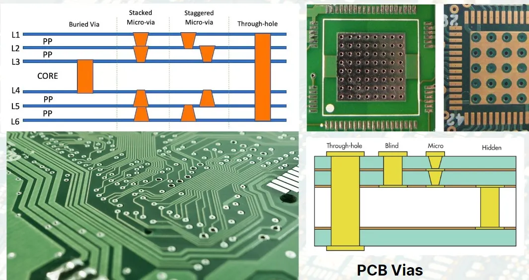
Understanding Sequential Build-Up PCBsSequential build-up PCBs are a type of multilayer board constructed through a step-by-step layering process. Unlike traditional multilayer PCBs, where all layers are laminated in a single step, SBU PCBs are built by adding layers sequentially, often using microvias to connect them. This method allows for higher layer counts, finer traces, and more precise control over the board's structure. The key advantage of SBU technology is its ability to support high-density interconnects (HDI), which are crucial for modern electronics with compact designs and high-speed requirements. By using microvias (tiny vias with diameters as small as 0.1 mm), SBU PCBs reduce signal path lengths and minimize parasitic effects, directly improving signal integrity.
Key Benefits of Sequential Build-Up PCBs for Signal IntegritySequential build-up PCBs provide several advantages that make them ideal for high-speed applications. Let's explore how these benefits translate into better signal integrity:
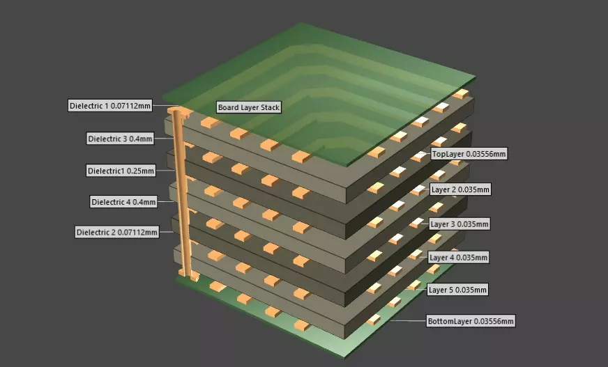
Signal Integrity Techniques Using Sequential Build-Up PCBsDesigning for signal integrity with SBU PCBs requires a combination of careful planning and proven techniques. Below are actionable strategies to optimize your high-speed PCB design: 1. Optimize Layer Stacking for Signal IsolationIn SBU PCBs, you have greater flexibility to design the layer stack-up. Place high-speed signal layers between ground planes to create a controlled impedance environment and shield against crosstalk. For example, a 10-layer SBU PCB might have signal layers at layers 2 and 8, with adjacent ground planes at layers 1, 3, 7, and 9. This configuration minimizes interference and ensures stable signal transmission at frequencies above 1 GHz.
2. Use Microvias to Minimize Signal DistortionMicrovias, a hallmark of SBU technology, are smaller and more precise than traditional vias. They reduce inductance and capacitance, which can distort high-speed signals. When designing, use stacked or staggered microvias to connect adjacent layers, keeping signal paths as short as possible. For instance, a microvia with a diameter of 0.1 mm and a length of 0.2 mm introduces far less parasitic inductance compared to a through-hole via spanning 1.6 mm across a board. 3. Control Impedance with Dielectric MaterialsImpedance mismatches are a leading cause of signal reflections in high-speed designs. SBU PCBs allow you to select specific dielectric materials with known properties, such as a dielectric constant (Dk) between 3.5 and 4.2 for common high-speed applications. Work with your PCB manufacturer to choose materials and layer thicknesses that maintain a consistent impedance, such as 50 ohms for single-ended signals or 100 ohms for differential pairs. 4. Minimize Crosstalk with Proper Trace SpacingIn high-density designs, traces carrying high-speed signals can interfere with each other if placed too closely. With SBU PCBs, you can achieve finer trace widths (down to 0.075 mm) and tighter spacing. However, ensure a spacing of at least 3 times the trace width between adjacent high-speed traces to reduce crosstalk. For example, a 0.1 mm wide trace should have at least 0.3 mm separation from its neighbor. 5. Implement Ground Planes and Power IntegrityA solid ground plane is essential for providing a low-impedance return path for signals, reducing noise and EMI. In SBU PCBs, you can dedicate entire layers to ground and power, ensuring minimal interruptions. Avoid splitting ground planes under high-speed signal traces, as this can disrupt the return path and cause signal degradation.
Challenges in High-Speed PCB Design and How SBU PCBs HelpHigh-speed PCB design comes with inherent challenges that can compromise signal integrity. Here’s how sequential build-up PCBs address these issues:
Best Practices for Designing SBU PCBs for Signal IntegrityTo maximize the benefits of sequential build-up PCBs in high-speed applications, follow these best practices:
Real-World Applications of SBU PCBs in High-Speed DesignSequential build-up PCBs are widely used in industries where signal integrity is paramount. In telecommunications, they support high-speed data transfer in 5G infrastructure, handling frequencies up to 28 GHz. In computing, SBU PCBs are integral to server motherboards and memory modules like DDR4, where data rates exceed 3.2 Gbps. Even in aerospace and defense, these boards ensure reliable communication in radar and avionics systems, where signal distortion can have critical consequences.
Conclusion: Elevate Your High-Speed Designs with SBU PCBsImproving signal integrity with sequential build-up PCBs is a game-changer for high-speed PCB design. By leveraging the precision of SBU technology, including microvias, optimized layer stacking, and controlled impedance, you can minimize signal distortion, reduce crosstalk, and ensure reliable performance in even the most demanding applications. Whether you're designing for telecommunications, computing, or aerospace, adopting signal integrity techniques with SBU PCBs will help you stay ahead in the fast-evolving world of electronics. Start by incorporating the strategies and best practices outlined in this guide into your next project. With careful planning and collaboration with your PCB manufacturer, you can achieve exceptional signal integrity and build circuits that meet the rigorous demands of modern technology. Share · · · · The Role of Flux in PCB Wave Soldering: Selection, Application, and Residue RemovalMarch 16, 2026PCB wave soldering flux types include rosin, water-soluble, and no-clean options with varying activity levels for oxide removal and solder flow. This guide covers selection criteria, spray foam drop-jet application methods, residue removal processes, and alternatives like nitrogen blanketing to boost joint reliability and yields for engineers. Article Achieving Uniform Solder Fillets in PCB Wave Soldering: Process ControlMarch 16, 2026Achieve uniform solder fillets in PCB wave soldering with process control strategies. Optimize flux, preheat, wave height, conveyor speed for consistent fillet shape, height, and wetting balance. Includes visual inspection tips and troubleshooting for reliable through-hole assemblies. Boost quality in production. Article Optimizing Conveyor Speed for Efficient PCB Wave SolderingMarch 16, 2026Learn PCB wave soldering conveyor speed calculation to manage dwell time, immersion depth, and throughput effectively. Electric engineers get practical steps, best practices, and troubleshooting tips for higher process efficiency and fewer defects in wave soldering operations. Article Understanding IPC Standards for PCB Surface Finishes: Ensuring Quality and ComplianceMarch 11, 2026Understand IPC standards IPC 4552 ENIG and IPC 4553 immersion silver for PCB surface finishes. Ensure compliance, enhance solderability, and prevent common defects to achieve reliable, high quality circuit boards. Article Miniaturization Challenges in PCB AssemblyMarch 11, 2026Navigate the complexities of high density interconnect PCB assembly and precise component placement. Learn to tackle miniaturization challenges, from tiny part handling to thermal stress, ensuring robust and reliable electronics. Article High Speed Routing Techniques: PCBMarch 11, 2026Master high speed routing in PCBs to ensure signal integrity and minimize electromagnetic interference. Learn essential techniques for robust designs, from controlled impedance to differential pair strategies. Prevent performance issues and achieve reliable electronics. ArticleGet Instant PCB |